S2C Limited.
S2C Limited.
Innovation

Chip Design Verification Methodology

Chip Design Verification Methodology

Chip designers do their best to use the latest cocktail of verification techniques and tools, and EDA companies continually innovate new verification tools, design flows, and pre-verified silicon IP, in a valiant effort to achieve the elusive goal of achieving chip design verification perfection.

Chip Design Verification Methodology
Prototyping
  • High performance and high density

  • Automatic partitioning

  • Deep trace debug

  • Flexible & powerful I/Os


01
Emulation
  • High capacity


02
Simulation
  • Flexibly design in various ways

  • Cycle and event driven mode

  • High speed simulation engine

  • Advanced modeling interface


03
Formal
  • RTL code analysis

  • Logic equivalent check

  • Vacuous assertion check

  • Verification progress and coverage measurement


04
Modeling
  • Architecture design

  • System performance analysis logic equivalent check

  • Virtual devices

  • IP modeling in early design stage


05

Verification Tool Comparison

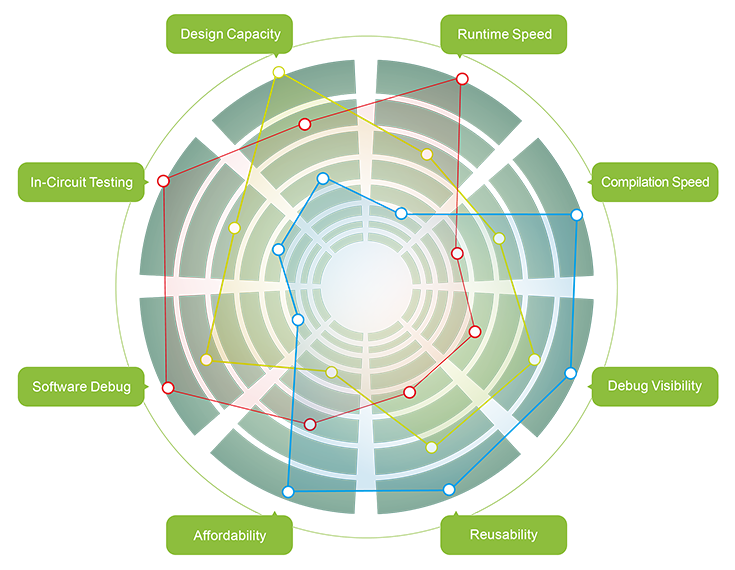
The increasing size and complexity of SoC/ASIC designs have led to an exponential increase in the complexity of validation. In order to reduce time to market, it is important to choose different verification tools in different design stages to improve efficiency and accelerate the convergence of verification.
All
Simulation
Emulation
Prototyping
S2C Verification Tool Comparison

Design Verification Process

Design Verification Process
Architecture Design
IP Development
SoC Integration
System Testing
Tape-out
Architecture Design
Simulation
Emulation
Prototyping
Formal
Heterogeneous Verification
Architecture Design
IP
Development
SoC
Integration
System
Testing
Tape-out
Rapid architecture design & System performance analysis & Software and hardware co-design
Shorten the Design Cycle

Heterogeneous Verification Platform

FPGA-based prototyping tools are scalable, cost-effective for almost any design, offer capable debug visibility, and are well suited to hardware-software co-verification. S2C has researched how the need for co-verification evolved with chip complexity, where FPGAs got their start in verification, and why ASIC design benefits from fpga verification methodology.
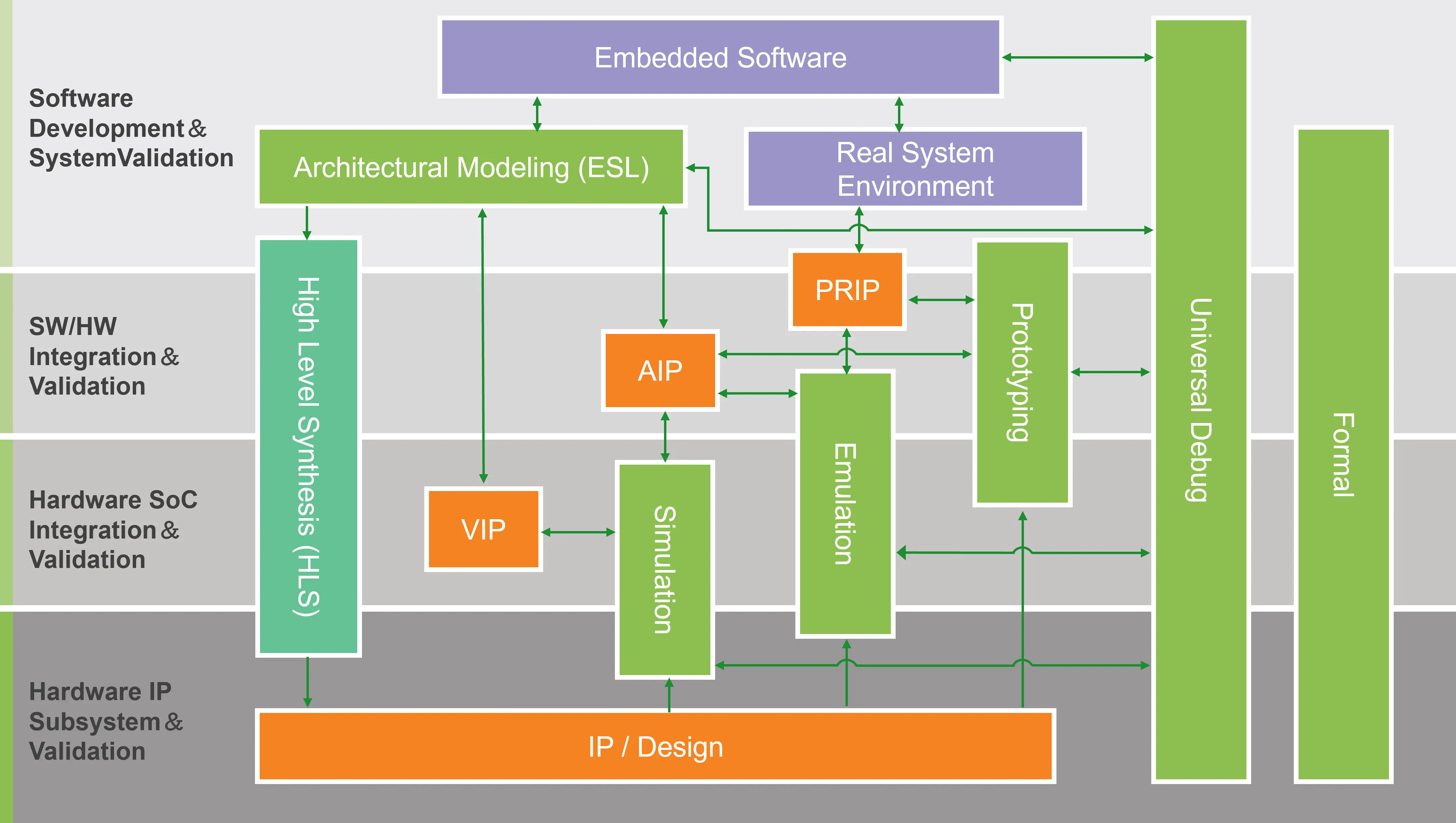
  • Design architecture planning, system performance analysis, virtualization application scenarios and IP modeling in the early stage

  • Support SystemVerilog, Verilog and VHDL RTL level simulation

  • Hardware simulation accelerates super-large design simulation speed and supports automatic compilation and full signal visibility

  • High-performance prototype verification for early software development and extensive system testing

  • Use transaction-level interfaces to reduce test program development time while ensuring the accuracy of system results

Heterogeneous Verification Platform
Request for Quote
What type of chip are you designing
What is the capacity of the ASIC gate included in the design?
5 million-20 million
20 million-50 million
50 million-100 million
100 million-1 billion
More than 1 billion
Which FPGA do you prefer to use?
Xilinx VU440
Xilinx KU115
Xilinx VU19P
Xilinx VU13P
Xilinx VU9P
Intel S10-10M
Intel S10-2800
Not sure, need professional advice
What kind of FPGA configuration do you need?
Single FPGA
Dual FPGA
Four FPGAs
Eight FPGAs
Not sure, need professional advice
What kind of peripheral interface do you need?
How many prototype verification platforms do you need?
Do you need the following tools?
Segmentation tool
Multiple FPGA debugging tools
Co-modeling tool (allows large amounts of data to interact between FPGA and PC host)
When do you need to use our products?
0-6 months
6-12 months
More than 12 months
Not sure
Any additional comments?