Visualization has taken full affect in today's modern world. We rely on video and images in every aspect of our lives from personal to industrial applications. Infotainment, gaming, medical, scientific visualization, security, mobile, finance, defense and the like all require extensive use of imaging. We depend so heavily on images, that image processing has become a vital industry. Today's video and static image processors must meet the finicky and in some cases mission critical demands of its users. Consumers of visual entertainment and gaming require unparalleled refinement in their images to reflect realism while the effectiveness of devices used in the medical and defense fields hinge on imaging to be extremely precise and communicated in real-time.
Video and static image processing in today's world has become enormously complex. Providers of this technology must design for such things as Bayer transformation, demosaicing, noise reduction and filtering, image sharpening, touch control, memory control and the speed in which these functions are performed and the final video/ image displayed.
These designs must also perform a huge number of DSP algorithms. Not only have the demands placed on the technology created complexity in the design, but also fostered a highly competitive landscape to say the least. In order for a vendor's technology to stay relevant, developers need to employ the most efficient and effective design and verification tools and methodologies. Graphic IP cores require a large number of test patterns to perform complete hardware verification and software testing. Furthermore, SoC designers who are planning to integrate complex IP cores such as image processors require a tremendous amount of verification effort such as verifying the correctness of all hardware functions, evaluating SoC bus efficiency and testing software capabilities.
![]()
It is very difficult for a computer to verify if the processing of a video or static image is correct or good enough. Verification is usually most effective when done by the human eye. Simulation is too slow to process images for proper human visual inspection to occur however, the rapid speed in which FPGA prototyping can run the design enables human verification of the image to be possible. Designers typically need multiple replicates to perform parallel testing making emulation too expensive. FPGA prototyping address this cost/efficiency issue head on as it is the only technology that can run the substantial amount of regression tests required fast enough and in the most cost effective manner. FPGA prototyping also has the unique ability to not only allow design teams to perform the necessary tests effectively and efficiently but also well ahead of silicon providing software developers much earlier access to fully functioning hardware.
Most image processing designs are large and require FPGAs that have the capacity to keep pace. S2C's series of Prodigy Logic Modules service a full range of design sizes up to 1.5 billion gates. Our wide variety of multimedia daughter cards for both HDMI and MIPI gives designs a faster way to construct their prototypes and run in-circuit testing while our design services team has the knowledge and experience to develop custom daughter cards to meet the discriminating needs of image processing designers. Having an easy-to-use and scalable rapid FPGA-based prototyping platform with a pre-verified graphics core on the platform significantly reduces integration pain on the SoC.
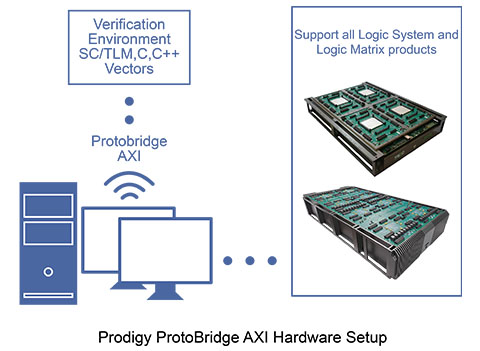
The use of S2C's patent-pending ProtoBridge™ System to perform transaction-based verification can significantly speed up the verification process with the ability to process imaging at full speed (up to 1000MB/s). This high-speed solution uses transaction-level interfaces to bridge the abstraction level between behavioral models and live hardware to enable communication between software running on a host and an FPGA-based prototyping platform that often includes memories, processors, and high-speed interfaces. ProtoBridge supplies a transactor interface between a software program and the world of AXI-compliant hardware. There are two key parts to this: an AXI-to-PCIe bridge that connects to a host computer, and a C-API that communicates to the design through the bridge. The software-to-AXI transactor offers new flexibility to designers building ARM-based systems. And coupling this to a PCIe interface, provides a perfect development platform for data-intensive applications.

A system like this allows designers to maximize the benefits of FPGA-based prototypes much earlier in the design project for algorithm validation, IP design, simulation acceleration and corner case testing.
S2C's entire Prodigy Complete Prototyping Platform provides solutions for every aspect of your design flow. We provide the most comprehensive array of prototyping logic modules to fit your design size as well as the largest library of pre-tested prototyping IP and reference design flows to speed up and simplify your prototyping process. Our Prodigy Cloud Cube™ is an enterprise-class, FPGA-based prototyping system that supports up to 32 FPGAs using a combination of Prodigy Logic Modules that allows prototyping to scale with the size of the design. The Prodigy Player Pro Software helps to configure the prototype and provides remote system monitoring and control. The compile functionality within Player Pro offers advanced partitioning and the soon-to-be-released Prodigy Multi-Debug System will relieve the arduous and error-prone task of debugging each FPGA manually. Another solution on the near horizon is our Neuro™ software that manages parallel/remote software development among distributed hardware and design teams. S2C's suite of Prodigy FPGA-based prototyping solutions is the most comprehensive on the market to help you realize the genius of your next design.