The Arm processor has become popular in recent years due to its versatility, energy efficiency, and widespread adoption across a wide range of devices. This popularity can be attributed to several key factors in the current market.
First and foremost, Arm processors are known for their power efficiency, making them ideal for mobile devices, IoT applications, and battery-powered gadgets. The architecture allows for efficient execution of instructions while minimizing power consumption, which extends battery life and reduces heat dissipation. Additionally, Arm architecture empowers chip manufacturers to tailor their designs to precise specifications, facilitating an optimal balance of performance, power efficiency, and feature sets. Moreover, Arm processors have demonstrated remarkable performance gains over the years, bridging the gap with traditional x86 processors, making them suitable for a broader range of computing tasks. These factors, combined with Arm's adaptability and scalability, have propelled its popularity and made it a dominant force in the world of microprocessors.
From smartphones to embedded systems, Arm processors find extensive use across various devices and applications, with interface IP serving as a crucial bridge for communication, connectivity, and data exchange. This drives continuous innovation in the technology sector. As a leading solution provider, S2C keeps up with the evolving trends in interface development during the high-performance computing era, helping developers address the challenges of high-speed data transfer.
When it comes to IP validation, a simulator which is low cost and easy to use is an attractive tool to choose. FPGA prototyping, on the other hand, could be a better solution if the IP is a part of a SoC which could benefit from being exercised by a processor core running software or real-world interfaces.
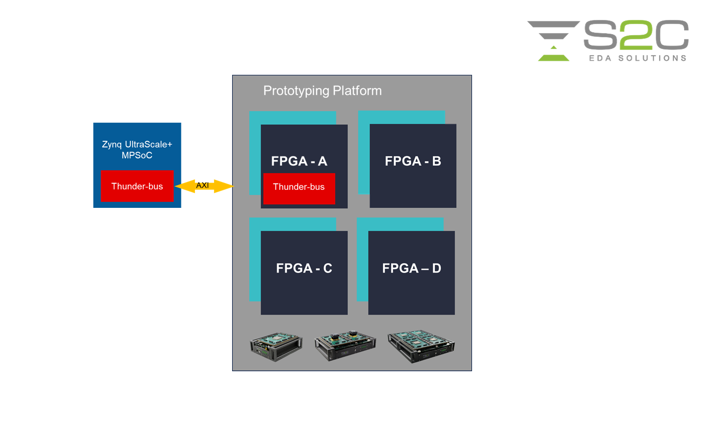
For example, an Arm's peripheral IP can be validated inside a Zynq UltraScale+ MPSoC, using the built-in hardcore Arm processor as an exerciser. Zynq UltraScale+ MPSoC provides an FPGA integrated with Arm cores and AXI structure interfaces, rendering it an optimal selection for low gate count validation purposes. However, due to its limited programmable gate count, bridging to a large FPGA is required when validating a mid-to-large size IP. Thunder-bus IP from AMD-Xilinx provides a chip-to-chip bridge to facilitate the linking of Zynq FPGA to another AMD-Xilinx FPA over AXI, with data rates up to 50Gbps. Xilinx ZC7(ZC702/ZC706/ZCU102) is a commonly used evaluation board Zynq UltraScale+ MPSoC development and S2C offers a Prodigy Zynq Interface Module to physically link ZC7 to Prodigy Logic System or Logic Module.

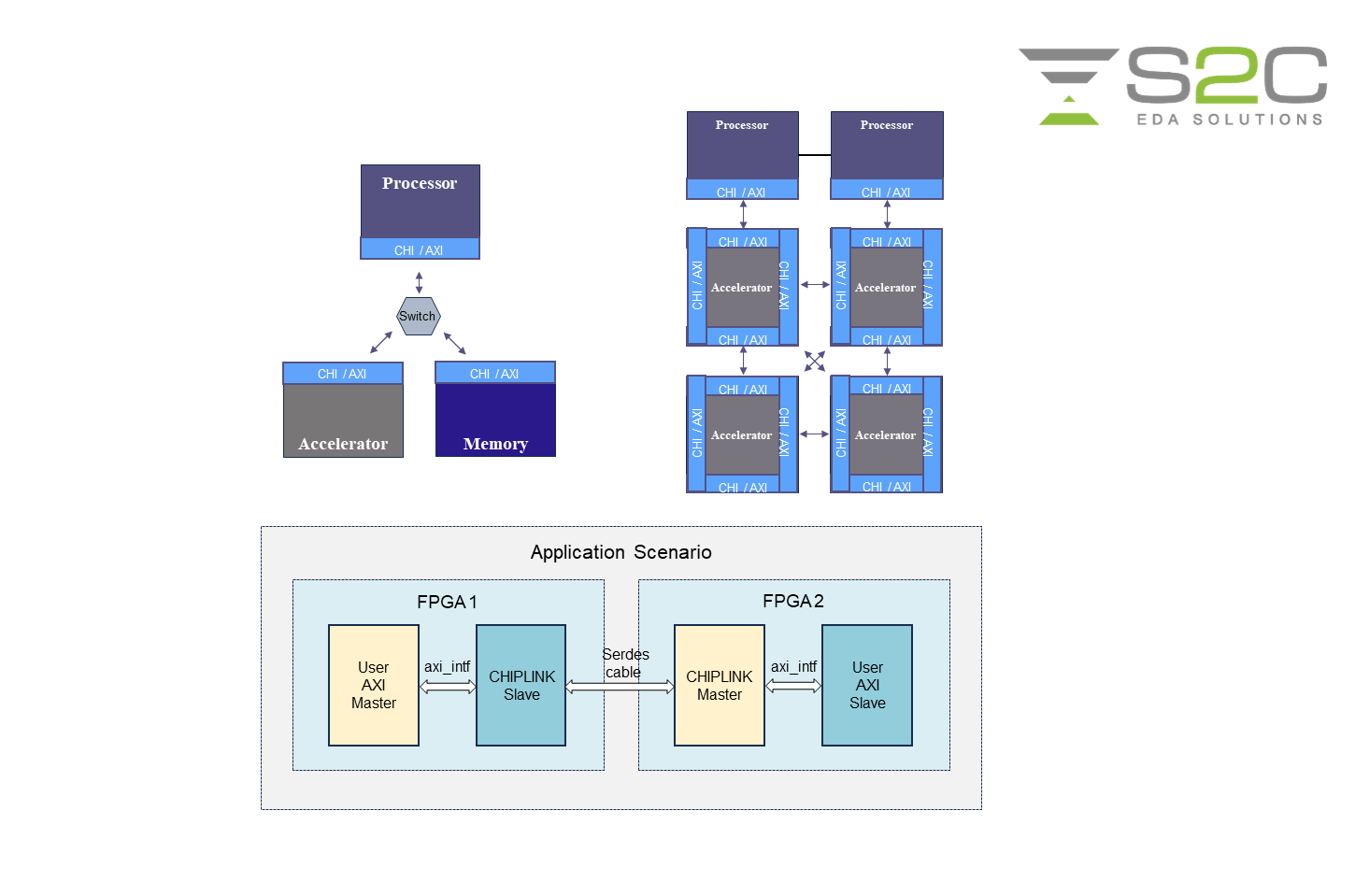
In addition to IP validation, such chip-to-chip IP is also very useful in partitioning an Arm based SoC design over multiple FPGAs at AXI boundaries. A typical partitioning using the traditional TDM method would drastically reduce the system operation speed to ~25MHz or lower; an AXI chip-to-chip based partition, on the other hand, supports multi-cycle operation over AXI and can still maintain a system speed of 50+ MHz.
Chiplink is an AXI chip-to-chip solution introduced by S2C, providing more features and higher performance. Chiplink supports up to 1024-bit AXI bus width, with each group able to accommodate up to 4 groups of AXI protocols per group. It also supports multiple Serdes line rates (12.5G/16.25G/20.625G/25G).

Another popular Arm-related IP from S2C is ProtoBridge. ProtoBridge is a high bandwidth AXI transactor over PCIe, enabling designers to maximize the benefits of FPGA-based prototypes early in the design project by providing a high performance data path between software running on a workstation and the AXI master/slave running in the FPGA prototype.
S2C's complete Prodigy FPGA prototyping provides effective assistance for your upcoming task. Contact S2C for more details on your next Arm design!