FPGA prototyping began with the introduction of FPGAs in the 1980s. It is a rapidly expanding market segment due to escalating chip and IP complexity and constricting window of opportunity. For competitive and developing markets, it is unquestionably essential to have your design confirmed rapidly and to provide hardware and software developers the chance to create, test, and improve their products concurrently.

A key concept in FPGA prototyping is using daughter boards because they provide flexibility. The limitation of test suites and internal FPGA boards provided by contemporary FPGA vendors is a typical problem. The fixed interfaces integrated on most evaluation boards often need to be improved for SoC/ASIC prototyping and are difficult to reuse in new projects. The same limitation applies to many home-grown FPGA boards, which are difficult to use in subsequent applications and rapidly as design specifications change. As a result, general-purpose FPGA prototyping systems are becoming more popular, making daughter boards a vital part of the solution.
What factors should be considered when choosing which FPGA prototyping system or daughter board to use? To use the daughter boards, the FPGA prototype system you select should have a lot of unused I/O pins on the I/O connections. The type of I/O connectors used by the system, how the pins are defined, the availability of different types of daughter boards, and the features that the FPGA board supports using daughter boards - so you don't need to build anything on it of your own - are the most crucial factors to consider when assessing a prototyping system in this regard.
When choosing an appropriate prototyping system, the quantity and kind of extension connections are crucial. Of course, the board's flexibility increases with the number of extension connections. But remember that when partitioning is required by design, the extension connections may also be utilized to connect FPGA boards. An excellent example is the FMC connection, which has a lot of commercially available daughter boards but is not the best option for general connectivity between FPGA boards due to its vast footprint and pin definitions. As an illustration, S2C's Prodigy Connector is a compact, high-performance, 300-pin connector that can support the running of multi-GHz transceivers. It supports three full FPGA I/O banks, and all traces from the same I/O connector have the same length. The Prodigy Connector has a matching Prodigy Cable that can connect 2 Prodigy Connectors with pin 1 matching pin 1. The Prodigy Connector supplies two voltages from the FPGA board to the daughter boards: 3.3V and VCCIO voltages.
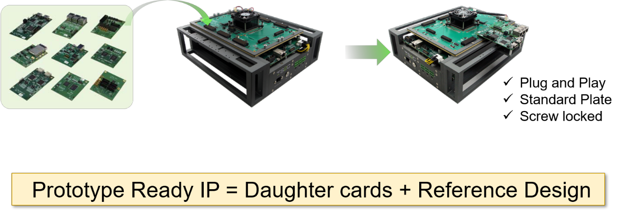
An extensive collection of pre-tested daughter boards helps decrease risks and conserve valuable engineering effort. The commercial daughter board may fulfill the criteria for many of the industry standards used by today's chip interfaces, including USB, HDMI, PCIe, Ethernet, DDR, and others. S2C has dozens of daughter boards covering processors, embedded & multimedia, high-speed GT, and memory applications. Take Prodigy 3 Channel RGMII/GMII PHY Interface Module as an example:
On the PCB or layout design stage, we have a rigorous design process to ensure the daughter board runs over 125MHz so that the Gigabit Ethernet can work well.
We implemented the auto-detection technology so that teams across the globe can remotely identify the presence of specific daughter boards and test it.
The IO voltage detection function is integrated, too. If somebody inputs a wrong voltage, the power will be automatically shut off to protect the hardware.
We also developed a reference design for it. Within this, a customer can quickly bring up their designs.
These daughterboards can be reused across multiple configurations of FPGA prototyping and among multiple projects/locations. The goal is to speed up and simplify customers' system prototyping process.
The ability of the FPGA prototyping provider to offer daughterboard modification services is another crucial factor to be taken into account. Many issues may be resolved using commercially available solutions, but unique system interfaces or optimizations are occasionally needed for SoC and ASIC applications. Therefore, customization services are helpful, especially if you're working on a project with a tight time-to-market deadline.