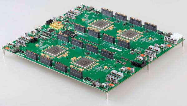
4th Generation System based on Altera Stratix IV FPGAs
San Jose, CA – April 21, 2011 – S2C Inc., a leading rapid SoC/ASIC prototyping solutions provider, announced its highest capacity SoC/ASIC prototyping system, the Quad S4 TAI Logic Module, based on four Altera Stratix IV 820 FPGAs. The Quad S4 TAI Logic Module can hold design up to 32.8 million gates and features S2C's fourth generation prototyping technology including enhanced power management, cooling mechanisms, noise shielding and convenient SD card download.
"This is an extension of our fourth generation technology first released in June 2010. We have shipped over 100 Altera Stratix IV-based dual and single S4 TAI Logic Modules in just nine months and we are pleased to offer the new Quad S4 to assist designers in prototyping even larger and more complex SoC/ASIC designs. Prototyping near real system performance is crucial in today’s design flow. This allows SoC hardware to be validated in real life and software developed concurrently. However many project managers have chosen not to prototype due to the difficulties in building/acquiring a multiple FPGA board that can meet their application/performance requirements that are reliable and easy to map a design into multiple FPGAs and debug. The Quad S4 TAI Logic Modules is designed to solve these issues and in addition, S2C’s TAI Player Pro 4.1 software release has been enhanced to support partitioning designs into four FPGAs”, said Mon-Ren Chene, Chairman and CTO of S2C.
"We are pleased to support S2C in developing their proven hardware boards that enable designers to rapidly develop Altera Stratix IV FPGA-based prototyping solutions featuring an unprecedented level of system bandwidth with superior signal integrity," said Phil Simpson, senior manager for software technical marketing and product planning at Altera. "We continue to partner with S2C to assist them in supporting our mutual customers."

Features
The Quad S4 TAI Logic Module contains a number of S2C's 4th generation features including:
High Capacity – up to 32.8 million gates per board with four Altera Stratix IV 820 FPGA devices
On board DDR2/DDR3 memory – Each board has two on-board DDR2 and two DDR3 SODIMM sockets to meet a variety of high speed memory applications.
1,920 Flexible I/O – Each FPGA has 480 I/O on four connectors and I/O voltage on each connector can be individually adjusted to 1.5/1.8/2.5/3.0V
Flexible Interconnect – 300 inter-connections among four FPGAs for SoC bus architecture. Additional Interconnects available through use of Interconnection Modules.
Design Partitioning – TAI Player Pro supports partitioning designs across four FPGAs
Advanced Clock Management – Nineteen global user clocks that can be choose from six software programmable clocks, three OSC sockets, three SMB connectors and ten feedback clocks.
Easy FPGA download – USB, SD Card, or JTAG
Comprehensive Self-Test program
Availability
The Quad S4 TAI Logic Module is available immediately. Contact your local sales representative for pricing information.
S2C's value is our singular focus on SoC/ASIC development. Our highly qualified engineering team and customer-focused sales force understands our customers’ SoC development needs. S2C’s unique FPGA-based solution, using our patented TAI IP technology, enables designers to quickly assemble FPGA-based SoC prototypes on S2C FPGA boards. This gives customers an early start on software development, typically the long pole item in development schedules. Combining rapid prototyping methodologies with a comprehensive portfolio of Prototype Ready IP and advanced verification and acceleration solutions, S2C solutions greatly reduces the SoC design cycle.
In addition to the headquarters in San Jose, CA, S2C currently has 4 direct offices located in Shanghai, Beijing, Shenzhen China and HsinChu, Taiwan. S2C is also the organizer of the annual SoCIP seminar and exhibition in China, which brings SoC designers from the Asia-Pacific region together with international silicon IP and SoC solution vendors.