Daniel Nenni Published on 09-03-2018 05:00 AM
FPGA Prototyping started with the advent of FPGAs in the 1980s and today it is a fast growing market segment due to increasing chip and IP complexities up against tightening windows of opportunities. Getting your design verified quickly and allowing hardware and software engineers the opportunity to develop, test, and optimize their products in parallel is critical for competitive and emerging markets, absolutely.
Working with S2C Inc. for the past few years has really been an eye opening experience in regards to FPGA Prototyping, Emulation, and the emerging Chinese fabless chip market. I will be writing a series of blogs based on my experiences with S2C in hopes of publishing a follow-on to our ebook "Prototypical" and this one starts with implementation and the importance of daughter cards.

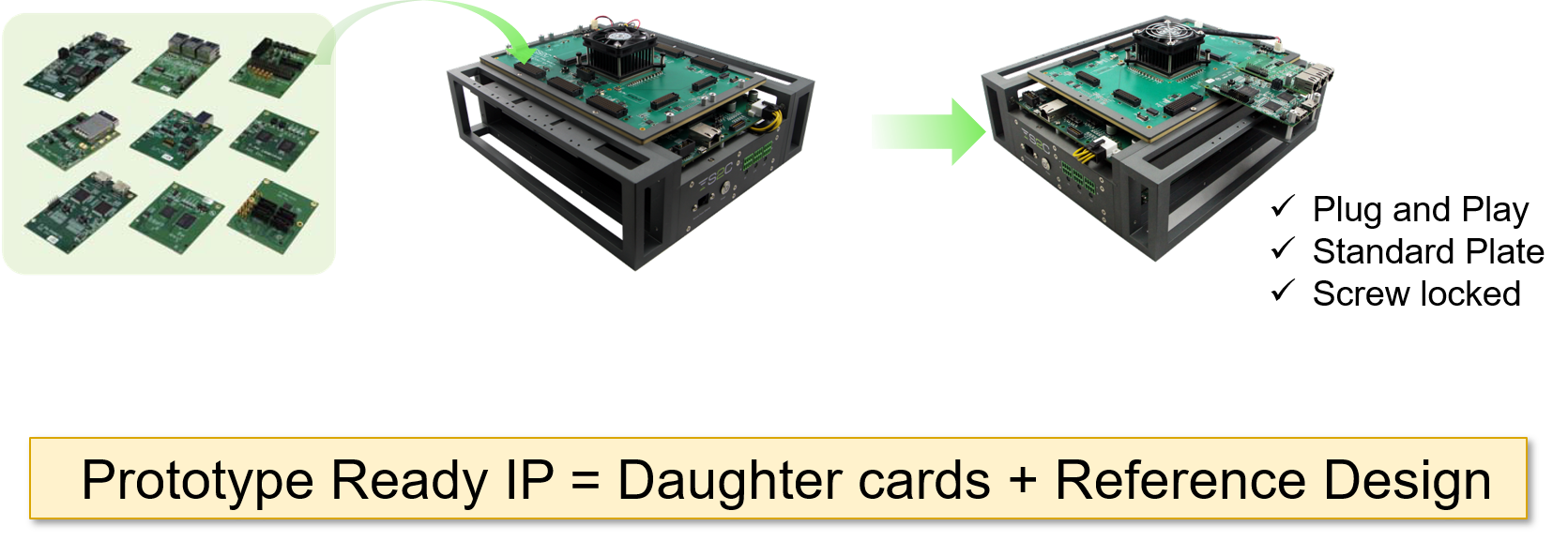
The use of daughter cards for FPGA prototyping is an important concept as it allows flexibility. A common problem is the limitations of current FPGA vendor's evaluation kits and in-house FPGA boards. Most evaluation boards have fixed interfaces embedded on the board which often cannot meet the SoC/ASIC prototyping requirements and is hard to reuse on new projects. Many home-grown FPGA boards also have the same limitation and easily get outdated when the design specification changes and they are hard to reuse for future projects. So more and more people choose general purpose FPGA prototyping systems making daughter cards a very important part of the solution.
S2C Interfaces and Accessories
What are the considerations for choosing daughter cards or the FPGA prototyping systems that will hold the daughter cards? Well, the FPGA prototyping system you select should have abundant unused I/O pins on I/O connectors in order to use daughter cards. Naturally, the most important methods for evaluating a prototyping system in this regard is to examine the type of I/O connectors the system uses, how the pins are defined, the availability of different types of daughter cards and what features the FPGA board supports for using the daughter cards, so you do not have to build anything on your own.
The number of expansion connectors and types are important criteria when selecting suitable prototyping hardware. Of course, the more expansion connectors there are on the board, the more flexible it is. But keep in mind that the expansion connectors may also be used to interconnect between FPGA boards when design requires partitioning. The FMC connector is a good example that has many off-the-shelf daughter cards but because of its large footprint and pin definitions, it is not ideal to use as general interconnect between FPGA boards. As an example, S2C's Prodigy Connector is a compact, high-performance, 300 pin connector that can support the running of multi-GHz transceivers. It supports 3 full FPGA I/O banks and all traces from the same I/O connector have the same length. The Prodigy Connector has a matching Prodigy Cable that can connect 2 Prodigy Connectors with pin 1 matching pin 1. The Prodigy Connector supplies 2 voltages from the FPGA board to the daughter board: 3.3V and VCCIO voltages.
A vast library of pre-tested daughter cards can save precious engineering time and reduce risks. Many of today's chip interfaces use industry standards, such as USB, HDMI, PCIe, Ethernet, DDR, and others, and the commercial daughter card can meet the requirements. S2C has dozens of daughter cards coverring processors, embedded & multimedia, high-speed GT and memory applications. Take Prodigy 3 Channel RGMII/GMII PHY Interface Module as an example:
On the PCB or layout design stage, we have a rigorous design process to ensure the daughter card runs over 125MHz, so the Gigabit Ethernet can work well.
We implemented the auto-detection technology, so that the teams across the globe can identify the presence of specific daughter cards remotely and test on it.
The IO voltage detection function is integrated too, if somebody inputs a wrong voltage, the power will be automatically shut off to protect the hardware.
We also developed a reference design for it, within this, a customer can quickly bring up their designs.
These daughter cards can be reused across multiple configurations of FPGA prototyping and among multiple projects/locations. The goal is to speed up and simplify customers’ system prototyping process.
Another key consideration is whether the FPGA prototyping vendor can provide daughter card customization services. Off-the-shelf solutions solve many problems but sometimes special system interfaces or optimizations for specific SoC and ASIC applications are required. So customization services can be extremely beneficial especially when you are working on a time-to-market critical project. S2C has had numerous customization services over the past 15 years, the typical SOW covers schematic design, PCB layout, SI simulation (optional), manufacture, hardware initial bring-up and test design develop and delivery. Even if you would prefer to build the daughter card in-house S2C can provide the daughter card design guideline and support to speed your efforts and reduce risk of delays.
About S2C
S2C, is a global leader of FPGA prototyping solutions for today's innovative SoC/ASIC designs. S2C has been successfully delivering rapid SoC prototyping solutions since 2004. With over 500 customers and more than 3,000 systems installed, our highly qualified engineering team and customer-centric sales team understands our users' SoC development needs. S2C has offices and sales representatives in the US, Europe, Israel, China, Korea, Japan, and Taiwan.
S2C, the S2C logo, Prodigy, MDM, MDM Pro, Logic System and Logic Matrix are trademarks or registered trademarks of S2C. All other trademarks are the property of their respective owners.
Media Contact
Amy Gong
MARCOM Manager
Email: marketing@s2ceda.com