Pre-Engineered Components Speed SoC Prototype Development and Reduce SoC Development Time
Shanghai, China – November 15, 2010 – S2C Inc., a leading rapid SoC prototyping solutions provider, announced that S2C customers can now buy DDR2 and DDR3 Prototype Ready IP that work with S2C’s 4th generation S4 TAI logic module. The Prototype Ready IPs enable customers to have out-of-box 2GBytes of DDR2 SDRAM operating at up to 533Mbps or 2GBytes of DDR3 SDRAM operating at up to 800Mbps on S2C’s Altera Stratix IV based FPGA prototypes. Getting FPGA DDR2 and DDR3 memories to run at these high frequencies requires significant engineering. S2C has pre-engineered these designs to allow engineers to quickly create SoC prototypes.
The DDR2 and DDR3 Prototype Ready IPs utilize the memory controllers supplied by Altera Quartus Software and have been pre-mapped and fine tuned to work at high-performance with selected DDR2 and DDR3 SO-DIMM memory tested by S2C. With the purchase, customer will get a TAI Player software project file, which has the entire reference design already mapped to S4 TAI Logic Module, and documentation giving step by step instructions on how to run the DDR2 or DDR3 memory. Customer can easily adjust DDR2/3 clock frequencies in the TAI Player software to verify that the read and write operations are correct at different clock speeds.
S2C’s DDR2 and DDR3 Prototype Ready IPs are useful reference designs to speed SoC development regardless of the actual memory controllers utilized in the final SoC implementation. S2C’s goal is to ensure that customers can first get their SoC prototypes with DDR2 and DDR3 external memory up and running in shortest possible time with Altera’s supplied memory controllers. If customers have needs to verify their designs with the actual memory controllers in the SoC, the settings in the Prototype Ready IP such as pin assignments, timing constraints and other Altera Quartus settings can then be used as references.
“Large external SDRAM memory is often a critical element in today’s digital system design and there is an ever increasing need to have a stable SoC prototype on FPGA with large high-performance DDR2 and DDR3 external memories,” said Mon-Ren Chene, S2C’s Chairman and CTO. “Running DDR2 and DDR3 at high-performance on FPGAs is not easy and if not engineered properly can lead to poor and unstable system performance. S2C’s DDR2 and DDR3 Prototype Ready Kits are pre-engineered to eliminate these potential problems. Our goal is to continue to provide our customers with pre-engineered solutions that will shorten the time to achieve a working SoC prototype resulting in shortened design cycle enabling our customers to beat their competition to market.“
DDR2 and DDR3 Prototype Ready IPs are now available on all S4 TAI logic modules. The S4 TAI Logic Module is S2C’s 4th generation SoC prototyping hardware which facilitates much higher system prototype performance and reliability through enhanced power management, cooling mechanisms and noise shielding. S4 TAI Logic Module can mount either one or two Stratix IV FPGAs and supplies up to 30 million ASIC gates of capacity and provides 1,286 external I/O connections on one board. Multiple TAI Logic Modules can be stacked or mounted on a interconnect mother board to meet even larger gate count needs.
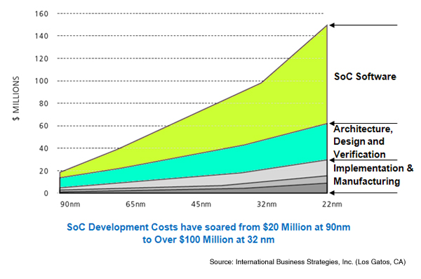
Rapid SoC Prototyping S2C focus is on reducing SoC development times via rapid SoC prototyping. Our vision is to provide the SoC developer the tools and building blocks to rapidly create and verify the functionality of the SoC. Once the functionality is verified, the hardware and software development can begin in parallel. Using the SoC prototype as a software development platform is not only orders of magnitude faster than computes simulation but can surface errors sooner since the software is running in real system conditions. This has a huge impact on SoC development schedules as software is increasing consuming SoC development resources. SoC development costs are soaring, but moreover the SoC Software development cost is the fastest rising cost. SoC Software is becoming the bottleneck for many projects as more functions are tightly integrated into a SoC and requires large number of engineers to develop and test software concurrently.

S2C's comprehensive system prototyping solution enables S2C’s customers to get to market ahead of their competitors.
About S2C
Founded and headquartered in San Jose, California, S2C has been successfully delivering rapid SoC prototyping tools since 2003. S2C provides:
Rapid SoC FPGA-based prototyping hardware systems plus design and verification software.
Third-party Prototype Ready IP™
SoC design, prototype and production services
S2C’s value proposition is our highly qualified engineering team and customer-focused sales force that understands our customers’ commercial SoC development needs. S2C’s unique FPGA-based electronic system level (ESL) solution, using our patented TAI IP technology, enables designers to quickly assemble FPGA-based SoC prototypes on S2C FPGA boards easily and securely. This enables customers to start software development, typically the long pole item in development schedules, immediately. Combining rapid prototyping methodologies with a comprehensive portfolio of Prototype Ready IP and advanced design solutions, S2C can reduce the SoC design cycle by up to nine months.
S2C currently has 3 direct offices located in Shanghai, Beijing and Shenzhen to meet the demand for accelerated SoC design activities in China. S2C is also the organizer of the annual SoCIP seminar and exhibition in China, which brings SoC designers/professionals from the Asia-Pacific region together with international silicon IP and SoC solution vendors. For more information, visit www.s2cinc.com.
Contacts for S2C:
Steve Pollock, S2C Inc., San Jose, Phone: +1 408 600-0547 Email:stevep@s2cinc.com
Michel Cao, S2C Inc., Shanghai, Phone: +86 21 6887 9287 Email:michelc@s2cinc.com
S2C, Prototype Ready and TAI, are trademarks of S2C, Inc. Altera and Stratix are registered trademarks of Altera Corporation. All other tradenames and trademarks are the property of their respective owners.