Enables High Speed Data Transfer between the FPGA-Based Prototype and the User's Verification Environment and Enables Simultaneous Debug of Multiple FPGAs
San Jose, CA – September 19, 2011 – S2C announced that its Verification Module Technology (patent pending) is now available for its Xilinx based FPGA prototyping systems. The V6 TAI Verification Module enables the high-speed transfer of massive data between the FPGA prototyping environment and the user's verification environment. Users can use their Xilinx ChipScope or 3rd party debug environments to view up to 4 FPGAs simultaneously. In addition, the V6 TAI Verification Module can be used to prototype designs from 1.3 million ASIC gates to 4.7 million ASIC gates. The V6 TAI Verification module provides high speed interfaces including PCIe Gen2, Gigabit transceivers, SATA2 and USB 3.0.
Mon-Ren Chene, S2C’s Chairman and CTO, said: “Our Xilinx based customers have requested our Verification Module technology that was first released in June of this year. This is breakthrough technology to interface the user’s FPGA prototype and verification environments. The simultaneous multi-FPGA debug gives users new important capabilities as designs are often split across multiple FPGAs. FPGA prototyping systems are running at system or close to system speeds. The high speed interfaces make it easier to connect the FPGA prototype environments to the actual target system environments.”
Three Modes of Operation
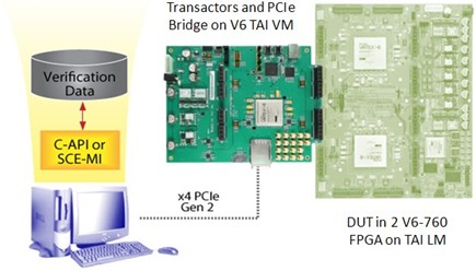
The versatile S2C V6 TAI Verification Module provides three usage modes: Verification Mode, Debug Mode and Logic Mode. The Verification Mode enables the transfer of large amounts of data from/to a PC through a x4-lane PCIe Gen2 interface using SCE-MI or customizable C-API. In the Debug Mode, the V6 TAI Verification Module enables simultaneous debugging of multiple FPGAs using Xilinx ChipScope or other 3rd party tools while maintaining the user’s RTL net names. The user can prototype a design with capacity up to 4.7 M gates in the Logic Mode. All debug and verification setup for the Verification Module is done in S2C’s TAI Player Pro™ software.
Verification Mode
The verification mode utilizes the TAI Verification Module's high speed PCIe Gen2 interface to rapidly and bi-directionally transfer large simulation data to and from the TAI Logic Module. This mode can be used to directly connect a prototyping system to a simulator for co-simulation. The user can utilize S2C-provided customizable C-API or can industry standard SCE-MI interface as shown in the following diagrams:

Debug Mode (Maximize Visibility)
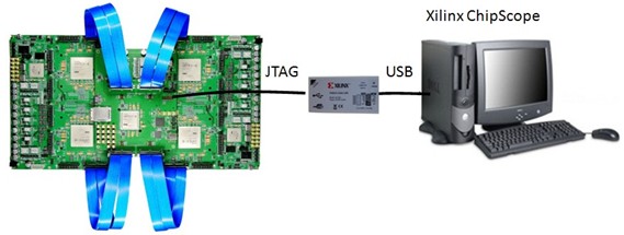
The Debug Mode utilizes the user's existing Xilinx ChipScope or other 3rd party debug environments. The V6 TAI Verification Module takes user defined signals from the multiple FPGAs in the Logic Module and sends them to the V6 TAI Verification Module where ChipScope is connected through the V6 TAI Verification Module's JTAG interface.
V6 TAI Verification Module can concurrently debug a 4 FPGA design in 2 Dual V6 TAI Logic Module.

120 signals from each Virtex 6 FPGA are routed to the V6 TAI Verification Module's FPGA. The user has the capability of routing 120 x N signals from up to 4 V6 FPGAs. For the initial software release, N is fixed at 4 but it will be user defined in future releases. All the user needs to do for set up are select probes in RTL level before design are synthesized and place them in different groups of 120 probes per FPGA, S2C's TAI Player Pro automates the multiplexing of pin data and route the debugging signals from multiple FPGA to a single Xilinx ChipScope in The V6 TAI Verification Module, while retaining the RTL names. The debugging data is stored in the V6 TAI Verification Module FPGA memory until preset trigger conditions cause it to be dumped for debug by Xilinx's ChipScope.
Logic Mode
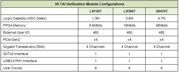
The V6 TAI Verification Module can be used as a standalone prototyping board for smaller scale SoC or ASIC designs for up to 4.7 M gate capacity. The V6 TAI Verification Module can utilize either the Xilinx LX130T, LX365T or SX475T FPGAs and has a total of 480 external I/Os on 4 LM connectors, x4 PCIe Gen2 Interface, 4 channels of Gigabit transceiver through SMA connectors, a SATA2 interface and a USB3.0 PHY Interface.
Configuration details are given in the following table:

Availability
The V6 TAI Verification Module hardware is available today.