Low Cost Enables Deployment of Multiple K7 TAI Logic Modules to Concurrently Accelerate SoC Designs
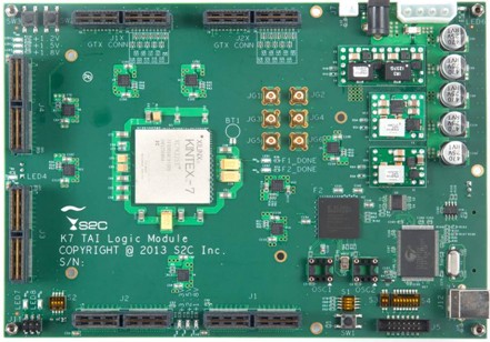
San Jose, CA – May 28, 2013 - S2C Inc., a leading rapid SoC/ASIC prototyping solutions provider, announced today a new family of its fifth-generation product, the K7 TAI Logic Module, based on Xilinx’s 28-nm Kintex-7 FPGA devices. The K7 TAI Logic Module provides up to 4.1 million ASIC gates of capacity, 432 external I/O and 16 channels of Gigabit Transceivers capable of running up to 10Gbps. K7 TAI Logic Module is shipped with TAI Player Pro runtime software and starts at an affordable list price.

“ FPGA-based prototyping is a critical step for a successful SoC product launch and project manager ideally wants every hardware and software engineer to have one prototyping system on their desks. But, the rising cost of high-end FPGA-based prototyping systems, which may easily run from $100K and upwards, greatly limits the number of available FPGA-based prototyping systems for a SoC project can deploy," noted Toshio Nakama, CEO of S2C. “ With less than one tenth the cost of a high-end FPGA-based prototyping system the K7 TAI Logic Module still provides a rich set of features for SoC and ASIC prototyping. The K7 TAI Logic Module allows project managers to deploy large number of FPGA-based prototypes for tasks like IP development, block-level verification, simulation acceleration, full SoC Verification and Software Development. Hardware design, system verification and software development processes can run concurrently to shorten overall project schedule.”
The K7 TAI Logic Modules adopt similar form factor to S2C’s high-capacity V7 TAI Logic Module with 1, 2 or 4 Virtex-7 2000T devices with capacity offering up to 80 million ASIC gates on a single board. Therefore, if a design outgrows the capacity of K7 TAI Logic Module, project managers can migrate to V7 TAI Logic Modules seamlessly. For larger SoC designs that cannot fit into a K7 TAI Logic Module, project managers can still utilize the K7 TAI Logic Modules for IP development, block-level verification, simulation acceleration and partial software development.
S2C K7 TAI Logic Module is equipped with many of S2C&lsquo's fifth generation technologies used on the flagship V7 TAI Logic Modules:
432 I/O on 4 dedicated I/O connectors with multiple voltages adjustable through runtime software in GUI
16 channels of GTX transceivers can run up to 10Gbps through 2 high-speed Differential I/O connectors
60+ off-the-shelf Prototype-Ready Interfaces and Accessories to quickly build the design prototype
Multiple FPGA configuration options: USB2.0 Port, JTAG and SD Card
Less than 1 second FPGA configuration through SD card
Runtime features are conveniently controlled from either Windows or Linux PC through USB ports including self-test, clock generation, setting I/O voltage, read hardware status
Multiple K7 TAI Logic Modules can be stacked or tiled to meet higher capacity need
The K7 TAI Logic Modules can run either 1GB of DDR2 or 1GB of DDR3 memory with pre-tested memory daughter cards. S2C offers a large library of Prototype Ready™ IP and accessories including High Speed D/A and A/D, PCIe, Gigabit Ethernet, MIPI, SATA, ARM, SRAM, DDR2/3, Flash, TV Decoder/Encoder, Audio and DVI to further accelerate user’s development of rapid FPGA based prototypes. In addition, S2C provides a complete solution with prototype creation and debug software; DPI, C-API and SCE-MI co-modeling.
Availability
K7 TAI Logic Module is now shipping with XC7K325T-2FFG900C or XC7K410T-2FFG900C FPGAs with a lead time of approximately 2 to 6 weeks. K7 TAI Logic Modules adopt similar form factor to all other TAI Logic Module families, so existing customers can easily upgrade and re-use their current daughter cards or mother boards.
S2C will be exhibiting the K7 TAI Logic Module at DAC 2013 from Monday, June 3rd to Wednesday, June 6th at booth #1925 at the 50TH Design Automation Conference (DAC) in Austin, Texas.
About S2C
Founded and headquartered in San Jose, California, S2C has been successfully delivering rapid SoC prototyping solutions since 2003. S2C provides:
Rapid FPGA-based prototyping hardware and automation software
Prototype Ready™ IP, interfaces and platforms
System-level design verification and acceleration tools
S2C's value is our singular focus on accelerating customer design cycle by providing FPGA-based design and verification methodology and tools. Our highly qualified engineering team and customer-focused sales force understands our customers’ SoC development needs. S2C’s patented FPGA-based technology enables designers to quickly assemble SoC prototypes. This gives customers an early start on software development, enabling concurrent hardware and software designs which are critical for modern day SoC. Combining rapid prototyping methodologies with a comprehensive portfolio of Prototype Ready IP, platforms and accessories, S2C solutions greatly reduces the SoC design cycle.