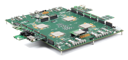
New product that supports 32GB on-board DDR3 memory and includes remote management features
Highlights:
Large capacity that accommodates up to 80M ASIC gates and supports up to 32GB on-board DDR3 memory
Powerful remote management capabilities through Ethernet that enable reading/writing the on-board SD cards, recycling powers and assigning I/O power-up sequences
San Jose, CA – February 25, 2014 - S2C Inc., a leading SoC/ASIC rapid prototyping solutions provider, is proud to introduce the newest FPGA-based prototyping platform to its V7 TAI Logic Module series, the QuadE V7. It is an enhanced version of the existing Quad V7 product which uses four Xilinx’s Virtex®-7 2000T FPGAs. The new QuadE V7 uniquely meets the needs of design groups working with large-capacity or high-performance DDR3 memory, which can support 8GB DDR3 memory on each of the four DDR3 SODIMM sockets with the pre-tested speed at up to 1600Mbps (Single Rank) and 1200Mbps (Dual Rank).
In addition, new remote management features on the QuadE V7 improve user experiences by allowing users to remotely perform operations through Ethernet such as reading/writing the on-board SD cards, re-downloading FPGA designs, recycling powers and assigning I/O power-up sequences. These new features empower companies to establish their common FPGA-based platforms across different locations, different projects and different design teams. A central group can now monitor all platform statuses, perform version controls of the design circuits, update design circuits, power down and re-start all deployed QuadE V7 prototyping systems through a company network.
QuadE V7 TAI Logic Module is available now for customer orders.
“FPGA-based prototyping is now used in our customer sites for a variety of purposes such as algorithm development, software development and compatibility testing”, said Toshio Nakama, Chief Executive Officer of S2C. “Therefore, the ability to remotely monitor and manage large numbers of FPGA-based prototypes deployed in different locations and groups has become a challenge for our customers. The new QuadE V7 was a result of our collaborations with key customers to enrich the remote management capabilities and help designers drive Prototype-On-The-Cloud one step closer to reality.”

About S2C V7 TAI Logic Modules
The V7 TAI Logic Module series, S2C’s fifth generation products, are designed to make prototyping a reality and a pleasant experience for designs ranging from 20 Million up to 80 Million ASIC gates on a single board. Multiple V7 TAI Logic Modules can be stacked or tiled to meet higher gate capacity requirements.
The V7 TAI Logic Module has many significant improvements that facilitate higher system prototype performance, reliability and ease-of-use. The V7 TAI Logic Module now supports the following hardware control functions through both the USB and Ethernet interface from a Windows or Linux machine:
Fast FPGA design download with multiple options – JTAG, USB, SD Card and Ethernet
Comprehensive Self-Test for all I/O, interconnections and clocks
Program clocks, select clock sources and adjust on-board programmable clock frequencies
Remote hardware control via Ethernet interface – Reset, configure FPGA design and execute run-time utilities
Monitor on-board voltage, current and temperature and automatically take corrective action upon limits violation
Read-back hardware information - global clock frequencies, hardware type, firmware details etc.
Adjust I/O voltages, FPGA cooling fan speed through software
Enables re-use of daughter cards designed for previous generation prototyping systems such as Virtex-6 or Virtex-5
TAI LM systems
S2C also provides optional prototype creation and multi-FPGA debug software, C-API co-modeling and a large library of off-the-shelf Prototype Ready IP & Accessories to speed up the creation of design prototypes using the V7 TAI Logic Modules. For more information, visit V7 TAI Logic Module product page on S2C website.
About S2C
Founded and headquartered in San Jose, California, S2C has been successfully delivering rapid SoC prototyping solutions since 2003. S2C provides:
Rapid FPGA-based prototyping hardware and automation software
Prototype Ready™ IP, interfaces and platforms
System-level design verification and acceleration tools
S2C's value is our singular focus on SoC/ASIC development. Our highly qualified engineering team and customer-focused sales force understands our customers’ SoC development needs. S2C’s unique FPGA-based solution, using our patented TAI IP technology, enables designers to quickly assemble FPGA-based SoC prototypes on S2C FPGA boards. This gives customers an early start on software development, typically the long pole item in development schedules. Combining rapid prototyping methodologies with a comprehensive portfolio of Prototype Ready IP and advanced verification and acceleration solutions, S2C solutions greatly reduces the SoC design cycle.
In addition to the headquarters in San Jose, CA, S2C currently has 4 direct offices located in Shanghai, Beijing, Shenzhen China and HsinChu, Taiwan. S2C is also the organizer of the annual SoCIP conference and exhibition in China, which brings together SoC designers from the Asia-Pacific region with international silicon IP and SoC solution vendors. For more information, visit www.s2cinc.com.
Contact for S2C:
Jimmy G. Chen, S2C, USA, Phone: +1 408 213 8818 Email: jxchen@s2cinc.com
Michel Cao, S2C, China, Phone: +86 21 6887 9287 Email: michelc@s2cinc.com
###
S2C, Prototype Ready and TAI, are trademarks of S2C, Inc. All other tradenames and trademarks are the property of their respective owners.