In EDA (electronic design automation), functional verification verifies that the logic design conforms to specification. Functional verification does not confirm the correctness of the design specification and assumes that the design specification is correct. It is one of the most challenging steps of the IC design cycle and is the main reason for IC re-spin.
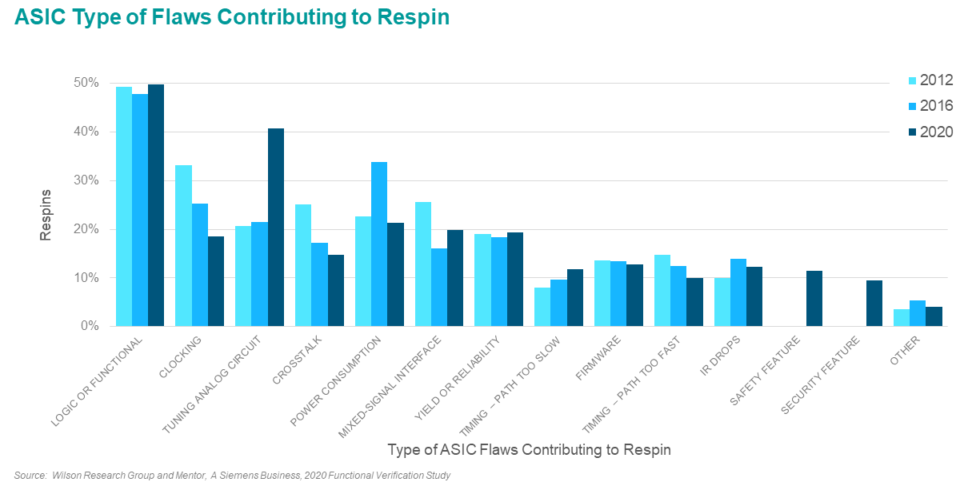
In the 2020 Wilson Research Group Functional Verification Study, figure 1 shows various categories of design flaws contributing to IC/ASIC re-spins, where the percentage of “logic or functional flaws” remains the leading cause of bugs.

Figure 1: Type of ASIC Flows Contributing to Re-spin
Functional verification can be attacked by many methods, but none of them are perfect. Each can be helpful in certain circumstances.
Logic simulation
Emulation
FPGA-based Prototyping
Formal verification
Functional correctness of individual IPs
Internal module communication
External module communication
End to end functional paths
Pad connectivity
Clock and reset circuits
Power up and down sequence
Complete integration of all IPs