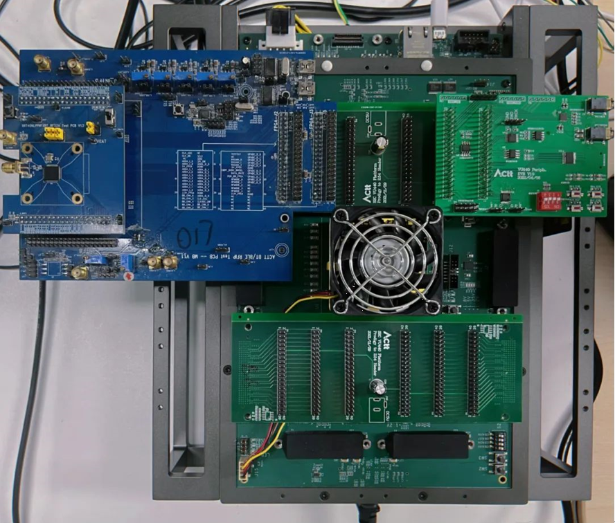
S2C has been shipping FPGA prototyping platforms for SoC verification for almost two decades, and many of its customers are developing SoCs and silicon IP for Bluetooth applications. Prototyping Bluetooth designs before silicon has yielded improved design efficiencies through more comprehensive system validation, and by enabling hardware/software co-design prior to silicon availability. When Bluetooth IP and SoC prototypes can be connected directly to real system hardware, running at hardware speeds, running real software prior to silicon, the resulting design efficiencies enable reduced development times, and higher quality products.
Bluetooth Low Energy (“BLE”) is a wireless communication technology that is used in a wide variety of applications including smart home devices, fitness trackers, and medical devices such as Neuralink's Brain-Computer Interface – applications that require low-power operation, and short-range wireless connectivity between devices (up to 10 meters). The Bluetooth protocol was originally introduced by the Bluetooth Special Interest Group (“Bluetooth SIG”) in 1998, followed by Bluetooth Low Energy (BLE) in 2009, and most recently the Bluetooth Low Energy Audio (“BLE Audio”) specification was released in 2022. BLE Audio focuses on higher power efficiency than the classic version of Bluetooth, provides for higher audio quality than standard Bluetooth, and introduces new features – and was the largest specification development project in the history of the Bluetooth SIG.
One provider company of silicon IP and SoC design services that chose S2C's FPGA based prototyping solutions for their SoC verification and system validation platform was Analog Circuit Technology Inc. (“ACTT”). ACTT was founded in 2011 and specializes in the development of low power physical IP and full SoC design services. ACCT's portfolio includes ultra-low power analog/mixed-signal IP, high reliability eNVM, wireless RF IP, and wired interface IP. ACTT's IP is widely used in 5G, Internet of Things (“IoT”), smart home, automotive, smart power, wearables, medical electronics, and industrial applications.
For one of its BLE projects, ACTT planned for a design verification and system validation platform that would take on several significant challenges;
1. A System-level Verification platform for a BLE Audio SoC that would enable comprehensive validation of the entire system's functionality, and would also support industry regulation compliance testing.
2. A Hardware/Software Co-Design platform that would provide the software development team with a platform for early software development and hardware/software co-design.
3. A Stability Testing platform – and as it turned out, several issues were surfaced by the verification platform that required highly-targeted debugging to ensure product stability and performance standards compliance.
Working together with ACCT on their BLE Audio project, ACCT selected S2C's VU440 Prodigy Logic System prototyping hardware platform, prototyping software, and debugging tools for a comprehensive FPGA prototyping platform. As part of their complete prototyping solutions, S2C offers a wide range of versatile daughter cards (“Prototype-Ready IP”), such as I/O expansion boards, peripheral interface boards, RF interface boards, and interconnect cables. S2C's Prototype-Ready IP supports prototyping interfaces for JTAG, SPI FLASH, UART, I2S, SD/MMC, and RF, with speeds of up to 60MHz. S2C's off-the-shelf Prototype-Ready IP enables faster time-to-prototyping, and reliable plug-and-play interconnection to S2C prototyping platforms.

Through committed collaboration with customer-partners, such as ACTT, S2C has a reputation for stimulating independent innovative thinking about SoC verification, and enhancing its customers' competitiveness in their respective markets. By working closely with its customer-partners, S2C fosters a thriving collaborative working environment that encourages the timely exchange of ideas, resources, and SoC development expertise. With a shared vision of success, S2C and its customer-partners strive to achieve successful SoC development outcomes like ACCT's, that delivers compelling value to our customer-partners.
S2C is a leading global supplier of FPGA prototyping solutions for today's innovative SoC and ASIC designs, now with the second largest share of the global prototyping market. S2C has been successfully delivering rapid SoC prototyping solutions since 2003. With over 600 customers, including 6 of the world's top 15 semiconductor companies, our world-class engineering team and customer-centric sales team are experts at addressing our customer's SoC and ASIC verification needs. S2C has offices and sales representatives in the US, Europe, mainland China, Hong Kong, Korea and Japan. For more information, please visit: www.s2cinc.com